By goodvin | 22 February 2024 | 0 Comments
Reduce Insertion Losses in PLC Chips With Waveguide Structure Optimizations
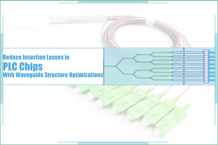
The increasing demand for high-speed data communication has pushed the development of photonic integrated circuits (PICs). Planar lightwave circuits (PLCs) are an important branch of PICs that utilize optical waveguides to route and modulate light signals on silica-based planar substrates. The waveguide structures are one of the fundamental components of PLC chips that determine their performance. By optimizing the waveguide design, the insertion loss, crosstalk, and other parameters of PLC chips can be significantly improved.
Bending waveguide structure
The bending regions of waveguides introduce additional loss due to mode mismatching, radiation loss, and scattering loss. A larger bending radius can reduce these losses but also occupy a larger chip area. Therefore, an optimized bending radius must strike a balance between loss and area efficiency.
Several techniques have been developed to reduce bending loss, including tapered waveguide bends, multimode interference bend structures, and adiabatic bends. These methods reshape the waveguide or vary the refractive index gradually along the bend to achieve an adiabatic mode transition that minimizes loss. With optimized bending structures, the loss of a single 90-degree bend can be reduced to below 0.01 dB.
Intersection waveguide structure
Waveguide intersections are essential for combining and splitting light signals in PLC chips. However, they can also lead to high insertion loss and crosstalk due to mode mismatching and scattering.
Some optimization techniques for waveguide intersections include:
Tapered waveguide junctions - The waveguide widths are gradually varied along the intersection to achieve an adiabatic mode transformation. This reduces reflection and scattering loss.
Multi-step waveguide transitions - Instead of a single continuous taper, multiple stepped tapers are used. This provides better control over the refractive index profile for lower loss.
Optimized intersection angles - Certain intersection angles can minimize mode coupling and scattering, resulting in lower loss and crosstalk.
Inverse taper waveguides - The waveguide widths increase away from the intersection, concentrating the optical field near the intersection to reduce crosstalk.
With optimized intersection structures, the loss can be reduced to below 0.05 dB and crosstalk below -25 dB.
Other optimization strategies
In addition to waveguide bends and intersections, other design aspects of the waveguides can be optimized to improve PLC chip performance, including:
• Reducing sidewall roughness through improved fabrication processes
• Varying the waveguide heights to control the refractive index profiles
• Utilizing shallow etch techniques to reduce scattering loss from sidewalls
• Optimizing the widths of straight waveguide sections
• Employing mode evolution optimizations along the entire length of the waveguides
All of these strategies work together to minimize waveguide propagation loss, which is critical for high-performance PLC chips. With thoughtful optimizations to the overall waveguide structure design, PLC devices with industry-leading performance metrics can be achieved.
keywords: waveguide optimization,PLC waveguide design, PLC bending loss reduction, PLC intersection loss reduction
FAQs
Q1: What is an optical waveguide?
An optical waveguide is a physical structure that guides light (in the form of electromagnetic waves) along a path. Optical fibers and the waveguides used in integrated optics are the two main types of optical waveguides. They confine and direct light through total internal reflection.
Q2: Why do waveguide bends cause loss?
Bends in waveguides cause loss due to several reasons:
Mode mismatching: The mode profile of the waveguide changes at the bend, causing a mismatch to the straight section after the bend. This results in reflection loss.
Radiation loss: Some of the light "leaks" out of the bend due to the changing mode, leading to radiation loss.
Scattering loss: Scattering from the sidewalls and imperfections of the waveguide contributes to loss, especially at tight bends.
Optimized bend structures aim to minimize these loss mechanisms.
Q3: What is an adiabatic waveguide bend?
An adiabatic waveguide bend is one where the mode transformation occurring within the bend is gradual enough that no optical power is coupled into higher order modes. This is achieved by slowly varying the waveguide width, height, or refractive index along the bend.
Since there is no sudden mode mismatch, adiabatic bends have extremely low insertion loss - theoretically unlimited for an perfectly adiabatic bend. However, in practice, scattering and imperfection losses still exist.
Q4: Why are tapers used at waveguide intersections?
Tapers are used at waveguide intersections to achieve an adiabatic mode transformation. Since the waveguides meet at an angle, their mode fields do not perfectly match.
By gradually varying the waveguide widths using a tapered structure, the mode fields can evolve slowly and overlap better, minimizing reflections and scattering at the intersection. This significantly reduces intersection loss and crosstalk.
Q5: What is the benefit of multi-step waveguide tapers?
Multi-step waveguide tapers, which contain multiple taper sections separated by straight sections, provide better control over the refractive index profile compared to a single continuous taper.
This is because each taper segment can be optimized independently to achieve the desired index profile for that region. The resulting field overlap and adiabatic mode transformation tend to be better than with a standard continuous taper.
As a result, multi-step tapers can achieve lower intersection loss and crosstalk compared to conventional single-step tapers.
Leave a Reply
Your email address will not be published.Required fields are marked. *